Hackaday · Creativity & design
Optically Altering Semiconductor Properties with Azo Compounds
Researchers have demonstrated a method to optically change the properties of semiconductor devices using azobenzene (Azo) compounds, potentially enabling dynamic adjustments to electronic behavior.
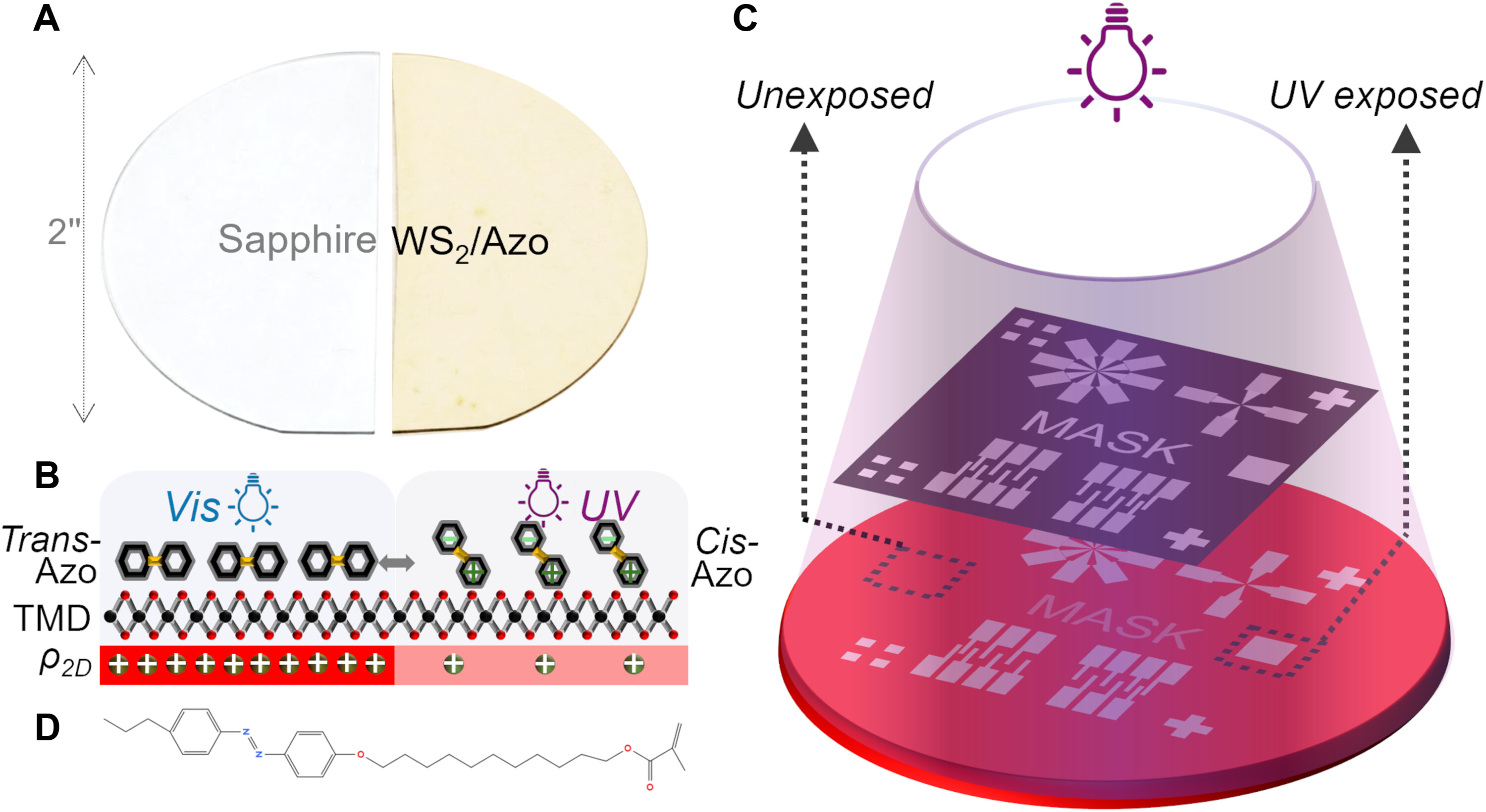
A study published in Science Advances by Jaehoon Ji et al. showcases the creation of a functional semiconductor device by integrating a transition metal dichalcogenide (TMD) monolayer with an Azo compound.
This integration allows the Azo compound to modify the electrical and optical characteristics of the semiconductor structure when exposed to UV light.
Experiments showed that both n- and p-type field-effect transistor (FET) semiconductors could have their carrier densities altered using visible and UV light, thereby changing the FET's behavior.
This proof-of-concept study suggests that semiconductor devices could be engineered to dynamically change their behavior in response to factors like electromagnetic radiation frequencies, electric fields, or temperature, by utilizing responsive Azo molecules.
The findings could open new avenues for developing programmable circuits and sensors.
AI-samenvatting op basis van de bron.
Hackaday