Hackaday · Creativity & design
DIY Double-Sided PCB Toner Transfer Method
A hobbyist has developed an improved toner transfer method for creating double-sided printed circuit boards (PCBs) at home, addressing the complexities of multi-layer fabrication.
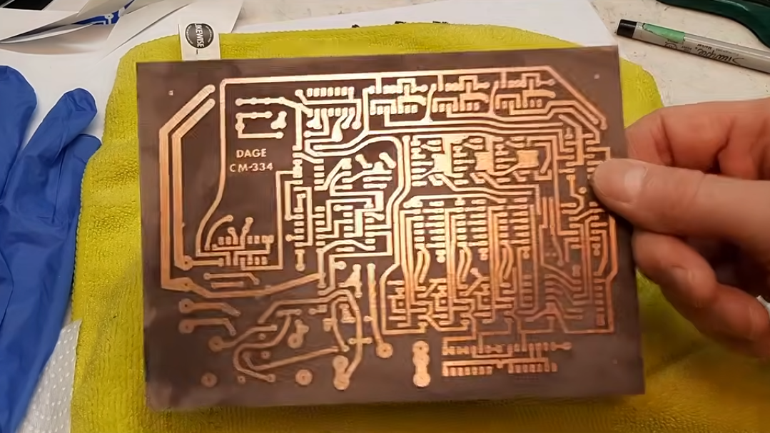
The method begins like a standard single-layer PCB process: toner is applied to a copper board and then etched in an acid bath. However, for a double-sided board, the second layer would be completely washed away during this initial etching.
To protect the second layer during the first acid bath, the inventor uses ink from a magic marker. After the first side is etched, the ink and toner are removed.
The second layer is then carefully aligned, passed through a laminator, and the opposite side is covered in ink before a second acid bath.
This process allows for the creation of a double-sided PCB at home, though the resulting board may be stained from the ink used.
The specific application for this custom PCB remains undisclosed, but it is likely related to antique electronics projects, a common theme in the inventor's work.
This method is particularly useful for hobbyists who prefer to fabricate their own PCBs at home rather than outsourcing to professional board shops, especially for unique or vintage-inspired designs.
AI-samenvatting op basis van de bron.
Hackaday